Currently Waiting for New Parts
Yesterday I placed an order for the parts that I was missing. This includes the 100Mohm resistor and a breakoutboard for my dac ic. The dac ic is a DAC8534, which has a tssop-16 package. I bought a conversion board for a ssop-48 package thinking that I could just leave out the extra pins (the 16 pin version came in a pack of 6 and was more expensive). This was however not the case as the tssop-16 proved to be too small to reach the pads.
Making a Custom PCB

The board to the left is what I planned to use for the preamp. It has solder pads in a repeated square pattern which gives you a lego-like freedom when placing components. This board in particular also has the same pitch as a SO-8 package so I can solder the opa129 op amp to it without any conversion board. For simple circuits like the preamp I like these prototyping boards since they allow you to be more hands on.
That being said these prototype boards are not without limitations. While they work well for most simpel things they are not great for sensitive stuff like RF or low current circuits. When dealing with very low currents you have to take a lot more things into account. For example the fact that small currents can leak through the pcb material and affect the signal. Since the preamp needs to measure low currents a custom PCB might be a better choice than this prototype board.
Since I was buying stuff i decided that I might as well design and order a custom pcb that will give me a better end result than the prototype board. It might require some extra patience but in the end I think it will be worth it.
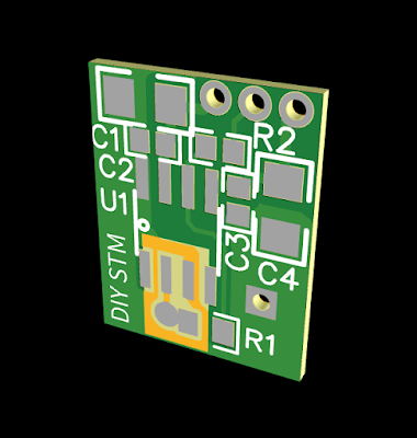
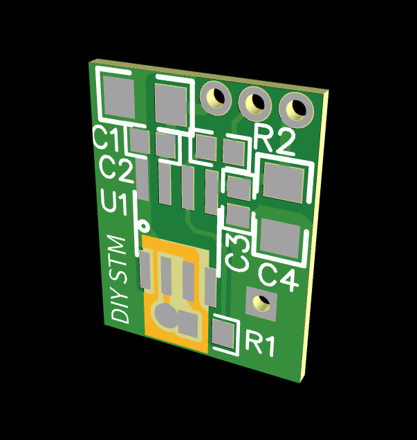
So after spending the week researching low current pcb design and learning EasyEDA I have designed the circuit board bellow.
EasyEDA is the software used to create this. It can also be used for other stuff like making schematics and simulating circuits. It would definitely have been convenient earlier in the project. That being said being able to do things manually is probably also something I value.
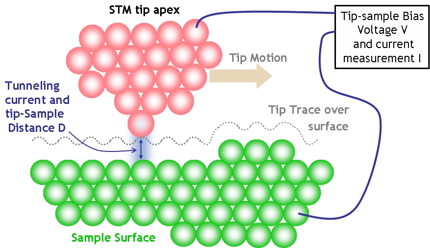
The yellow square is a guard ring that encloses the low current input. These are used in many circuits that handle very small currents. The guard ring is driven close to the same voltage as the input signal (in this case ground) and has a low impedence path to ground. This way very little current can leak to the input node. External currents simply leak into the guard trace instead.
I also designed the tssop-16 conversion board for the DAC8534 with this program. These boards cost less that the conversion board readily available.
In the Meantime...
Since I'm waiting for these circuit boards I can't really experiment with the DAC or the preamp. Both use a surface mount IC that can't be placed in a solderless breadboard is hard to desolder. I did however find some opamps at school with relatively low input bias currents. They will be enough for me to experiment with for the time being.